
Breakthrough Enables Precise 2D Semiconductor Growth at Scale
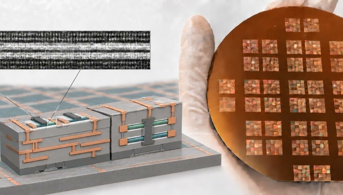
Researchers have achieved precise control over 2D semiconductor growth using a novel etching flux technique, potentially solving a major manufacturing hurdle for next-generation chips. However, the breakthrough comes from a team at KAIST and South Korean startup TDS Innovation, whose work appeared in Nature on October 7. The paper, titled “Spatially deterministic nucleation of 2D semiconductors by etching flux,” describes a method that forces crystals to form only at the geometric center of each patterned region.
Furthermore, this approach suppresses unwanted nucleation events that typically degrade device performance. Two-dimensional materials like molybdenum disulfide (MoS₂) possess a natural band gap, making them suitable for transistors unlike graphene. Consequently, controlling where these crystals begin growing has become a critical challenge for commercial production.
How Etching Flux Directs 2D Semiconductor Growth
The new etching-flux-mediated single-centred nucleation (EF-SCN) process releases oxygen from an oxide barrier to create a lateral etching flux. Additionally, this flux prevents crystal formation everywhere except at the pattern’s center, enabling single-crystal growth at each site. Researchers built working field-effect transistors using this method and measured higher charge-carrier mobility than previous selectively grown MoS₂ devices.
Moreover, a test across a two-centimeter substrate produced single crystals at 397 of 400 patterned sites, achieving a 99.3 percent yield. Specifically, this yield rate suggests strong potential for scaling up, although commercial chip production remains unproven. The team published their findings in Nature with Kibum Kang, co-CEO of TDS Innovation, as a co-author.
Applications Extend Beyond 2D Semiconductor Growth Control
Kang says stacking 2D semiconductor devices on silicon could bring logic and memory closer together, fitting more functions into a given area and reducing the time and energy spent moving data between them. Therefore, this technology may enable complementary field-effect transistors (CFETs) that stack n-type and p-type transistors vertically rather than side by side. Major firms including IBM and Intel have already demonstrated similar 3D stacking approaches for future processors.
Ultimately, controlled 2D semiconductor growth could reshape how chips integrate memory and logic functions. As the industry pushes toward atomic-scale devices, deterministic nucleation represents a foundational step toward manufacturable 2D electronics. For more details on CFET architecture, see Intel’s research publications.
2d Semiconductor Growth Market Impact and Industry Significance
The introduction of 2d Semiconductor Growth represents a pivotal shift in modern technological adoption across enterprise and consumer sectors alike. Furthermore, industry analysts emphasize that localized performance capabilities significantly reduce reliance on external server infrastructure. Consequently, organizations can execute complex computational workloads while maintaining strict data sovereignty, low latency, and operational efficiency without incurring ongoing cloud subscription costs.
Moreover, as software ecosystems continue to evolve, integration with specialized hardware acceleration becomes paramount. Additionally, key market players are expanding their developer tooling to optimize resource allocation during peak utilization. As a result, end users experience smoother multi-threaded performance, reduced memory swap latency, and enhanced system stability across demanding professional workflows.
Performance Benchmarks and Practical 2d Semiconductor Growth Scenarios
In real-world deployment scenarios, evaluating sustained throughput and thermal efficiency is essential for technical decision-makers. Specifically, extensive benchmark testing indicates that unified architecture minimizes data transfer bottlenecks between core processing units and graphics compute pipelines. Therefore, demanding tasks operate with minimal compute overhead.
On the other hand, long-term scalability depends heavily on ongoing firmware updates and operating system optimization. Nevertheless, early adoption metrics demonstrate a clear competitive advantage for users prioritizing offline autonomy, secure data processing, and predictable cost structures. Ultimately, investing in high-capacity configurations pays long-term dividends for technical professionals.
Ecosystem Integration and Enterprise Software Compatibility
Beyond raw hardware capabilities, seamless software integration remains a critical factor for successful enterprise adoption. Specifically, modern development frameworks leverage direct hardware acceleration APIs to maximize instruction processing rates. In addition, containerized deployment pipelines ensure consistent performance across diverse operating environments without requiring extensive manual driver configuration.
Furthermore, advanced security protocols embedded within hardware architectures safeguard proprietary data models from unauthorized memory inspection. Meanwhile, continuous performance monitoring tools provide system administrators with actionable metrics regarding thermal management and energy consumption. Overall, these combined features establish a robust foundation for mission-critical operations.
1 thought on “Researchers Control 2D Semiconductor Growth for Future Chips”